Overview

Fig. 1. Novel materials for future society
Electronic devices such as PCs and mobile phones are playing one of the most essential roles in the modern society. Those devices are based on electronic materials with diverse functionalities. A lot of researchers are currently working in the field of electronics in order to achieve further high performances.
In Fukumura group, we develop new functional materials using the cutting-edge techniques of solid state chemistry, especially focusing on nano-scale thin-film technology which is a foundation of many electronic devices. Our activities cover a broad range of research topics including design of novel functional materials, synthesis of solids with unusual crystal structures, measurements on electric/magnetic/optical properties and construction of new frameworks to understand newly found phenomena. We introduce some parts of our studies in this web-page.
Synthsis and development of functionalities for rare earth monooxides
Click here for details.
[1] K. Kaminaga, R. Sei, K. Hayashi, N. Happo, H. Tajiri, D. Oka, T. Fukumura and T. Hasegawa, Appl. Phys. Lett. 108, 122102-1-4 (2016).
[2] Y. Uchida, K. Kaminaga, T. Fukumura, and T. Hasegawa, Phys. Rev. B 95, 125111 (2017).
[3] K. Kaminaga, D. Oka, T. Hasegawa, and T. Fukumura, J. Am. Chem. Soc. 140, 6754 (2018).
[4] K. Kaminaga, D. Oka, T. Hasegawa, and T. Fukumura, ACS Omega 3, 12501?12504 (2018).
[5] T. Yamamoto, K. Kaminaga, D. Saito, D. Oka, and T. Fukumura, Appl. Phys. Lett. 114, 162104 (2019).
[6] D. Saito, K. Kaminaga, D. Oka, and T. Fukumura, Phys. Rev. Mater. 3, 064407 (2019).
Development of physical properties in layerd oxide R2O2Bi (R: rare earth metal) wtih Bi square nets
Click here for details.
[1] R. Sei, S. Kitani, T. Fukumura, H. Kawaji, and T. H. J. Am. Chem. Soc. 138, 11085 (2016).
[2] K. Terakado, R, Sei, H. Kawasoko, T. Koretsune, D. Oka, T. Hasegawa, and T. Fukumura, Inorg. Chem. 57, 10587 (2018).
Scanning tunneling electron microscope
準備中。
Transition Metal Oxide
準備中。
Mist chemical vapor deposition
準備中。
High-temperature ferromagnetic semiconductor (Ti,Co)O2
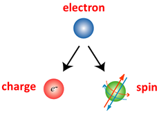
Fig. 2. Spintronics
Most electronic devices uses the features of semiconductors in which electrical conductivity can be controlled. Recently, development of semiconductors with some extra properties is required to add new functionalities to devices. One of such properties is ferromagnetism. Ferromagnets are materials with spontaneous magnetisation (i.e. conventional magnets) and its direction can be tuned by external magnetic field. "Spintronics", a new research area to use electical and magnetic properties in combination, is expected to enable development of next-generation devices.
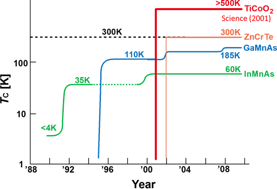
Fig. 3. Ferromagnetic semiconductor timeline
In ferromagnets, sponataneous magnetisation decreases with increasing temperature and finally vanishes at a critical temperature (Currie Temperature). When materials are used in electronic devices, they must work under nomal circumstances (room temperature: about 300 K). Room-temperature ferromagnets are usually limited to metals such as Fe, Co, Ni and alloys and most ferromagnetic semiconductors such as GaMnAs and InMnAs possess too low Currie temperature to be applied to room-temperature devices. Contrastively, (Ti,Co)O2, discovered by us, is a ferromagnetic semiconductor with quite high Currie temperature over 500 K is a solutino to this isuue and now regarded as a guide post of semiconductor-based spintronics[1].
Recently we succeeded in observation on microscopic magnetic domains in (Ti,Co)O2 with magnetic force microscopy[2]. In previous studies, magnetic domain observation was not achieved due to poor sample quality and/or too small magnetization of samples. In order to overcome the problems, we established the way to improve sample quality with self-buffer method[3]. The samples obetained with this method showed clear domain structure in sub-micron scale. These result would contribute to understanding and promoting ferromagnet-based devices such as ferromagnetic field effect transistors and current induced domain wall motion devices.
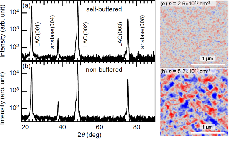
Fig. 4. Synthesis of high qualith thin films with self-buffer method (left) and micro scale domain structure in (Ti,Co)O2 thin film (right).
[1] Y. Matsumoto, M. Murakami, T. Shono, T. Hasegawa, T. Fukumura, M. Kawasaki, P. Ahmet, T. Chikyow, S. Koshihara, H. Koinuma, Science, 291, 854 (2001).
[2] T. S. Krasienapibal, S. Inoue, T. Fukumura, T. Hasegawa, Appl. Phys. Lett., 106, 202402 (2015).
[3] T. S. Krasienapibal, T. Fukumura, Y. Hirose, T. Hasegawa, Jpn. J. Appl. Phys., 53, 090305 (2014).
Novel synthesis route of a unnomal valent Y2O2Bi
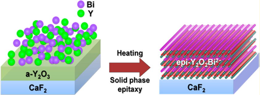
FIg. 5. Synthesis of Y2O2Bi with reductive solid phase epitaxy
Layered compouds are one of the most important group of functional materials because of their tremendous properties such as high temperature superconductivity of copper-based oxides. They play inevitable role in the field of electronics which relates to our life because their physical properties can be flexibly controled by changing the structure and/or chemical composition of each layer. Recently, spintronics using layered compounds has been promoted toward the development of low energy devices. Especially, Bi-based compouds are gathering much attention due to its high spin-orbital interaction, a key to control spins.
We focus on layered oxides R2O2Bi (R = rareearth metal and Y). Bi contained in R2O2Bi is in -2 valence, an unnomally reduced state, and forms 2 dimensional square-net atomic layers. In layered compounds based on Bi square nets, many intriguing properties have been reported including superoconductivity, conduction of zero mass Dirac electrons and giant magnetoresistance. R2O2Bi is expected as a topological material (topological insulator/superconductor) which can be used in next-generation spintronics. In order to extract these intrinsic properties, specimens in single crystal form are required. However, only polycrystalline samples have been available in pevious studies because of the difficulty in treating volatile and unnomal valent Bi.
We developed a novel synthesis method called reductive solid phase epitaxy and suceeded in preparation of single-crystal spcimens of Y2O2Bi for the first time[1]. This is a unique method using amorphous thin films and mixed powder of Bi and Y metals as precursors. What is important in this method is that Y metal works as a strong oxidant and, at the same time, prevents vaporization of Bi by forming alloy. This method is applicable for other series of R2O2Bi. We are now conducting detailed investigations on the physical properties of the obtained films, which would offers a new avenue to understand and develop new physics based on the annomal Bi square nets.
[1] R. Sei, T. Fukumura, and T. Hasegawa, Cryst. Growth Des. 14, 4227 (2014).
